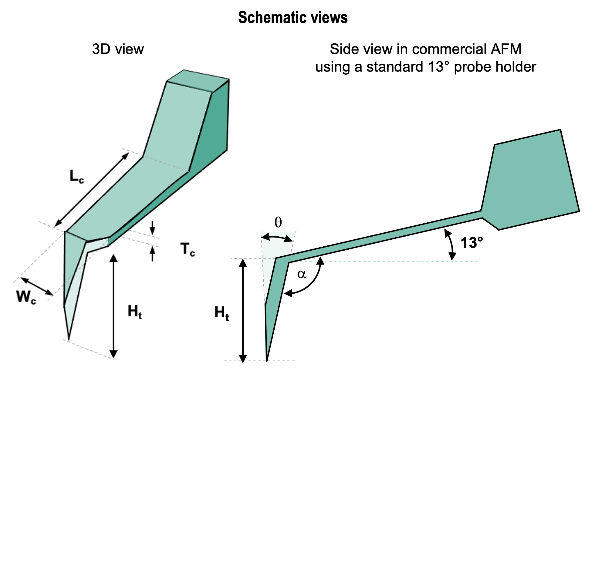













3D schematic of Vmicro TE003 A2-A2 30 AFM probe for TERS and tip-enhanced spectroscopy

Features

  • New MEMS technology
  • Long tip: extends AFM capabilities
  • Highly profiled tip with angle engineering
  • Tip visibility provides accurate landing
  • Vertical sidewall chip for safe handling

Applications

  • Tip Enhanced Raman Spectroscopy
PackagingPrice & quantity
Metal Box of 10 AFM Probes

High-quality gel-free packaging
unit price 75€
High-quality gel-free packaging
unit price $85

750,00 
→ You can generate a quote directly from the cart page
Order code : TE003_A2-A2_30

Specifications

3D schematic of Vmicro L400 AFM probe for Lprobe tapping mode
Parameter
Unit
Nominal
Range
Frequency
kHz
90
50-150
Spring constant
N/m
3
1-8
Tip height Ht
µm
30
15-50
Tip apex radius
nm
70
40-80
Tip side angle θ
°
15
+/- 0.5
Tip-cantilever angle α
°
118
+/- 0.5
Cantilever length Lc
µm
115
+/- 1
Cantilever Width Wc
µm
40
+/- 1
Cantilever Thickness Tc
µm
1.4
+/- 0.5
Cantilever backside coating
Au for optical modes
Tip side coating
Au for optical modes
Tip and cantilever material
p-type Silicon 0.01-0.02 ohm-cm
Chip dimensions
mm
3.4x1.6x0.4

Cantilever & tip details

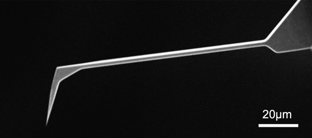
SEM full-view image of Vmicro TE003 A2-A2 30 AFM probe showing complete probe geometry
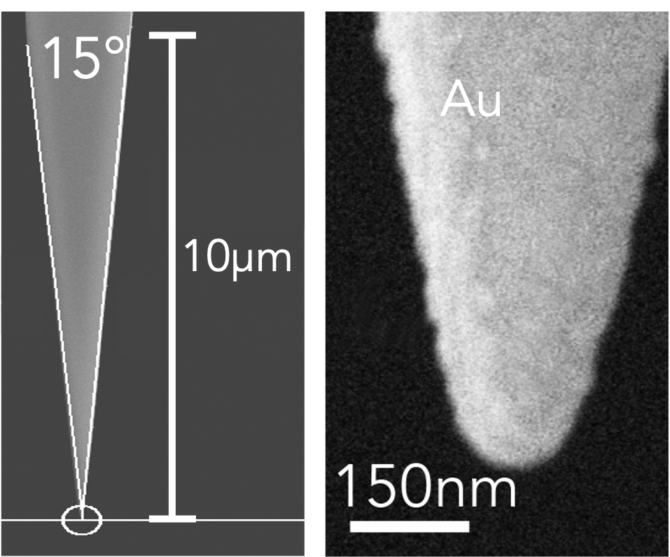
TERS AFM tip image with two panels: left 30 µm tip profile, right apex zoom (75 nm).
  • Tilted tip design
    Compensates for the AFM head mounting angle, ensuring accurate data on diverse sample surfaces.
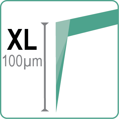
  • Tip height >30 µm
    Optimal optical access for TERS
  • Half-cone angle < 10° over the last 10 µm 
    Minimizes tip-sample convolution, ensuring more accurate morphological measurements.
  • Coating for spectroscopy
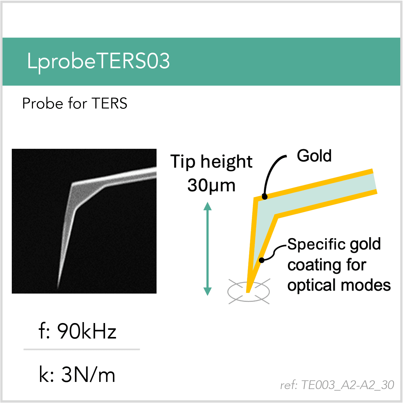
    Thick gold layer all faces of the tip, typical apex radius is 75nm. The coating is optimized for TERS measurement

Special packaging

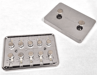
Spectroscopy and images with SNOM tips that have been packaged in standard AFM Gel-Pak boxes can lead to artifacts in the optical response. This is due to contamination of the tip by a few molecules of the gel. Vmicro has developed a back-end process with special decontamination and storage in a metal box. You can select this feature as an option when selecting your reference.



Nano-FTIR spectra normalized and obtained at the SMIS beamline at Synchrotron SOLEIL. (Courtesy F. Borondics – G. Németh)

Find probes by application

Conductive

Electrical measurements

s-SNOM

s-SNOM Probes for IR

Platform Cantilevers

Tilt compensated flat surface