LS003_Si-Si_30

Features

  • New MEMS technology unlocking probe engineering
  • Long tip with profiled shape
  • Low cone angle
  • TrueTipView: Precise tip visibility thus accurate landing on sample
  • Vertical sidewalls probe chip for easy handling

Applications

  • Topography imaging in
    • Soft tapping mode
    • Force modulation mode
  • Roughness measurements
  • Nanoscale imaging on highly corrugated samples
  • Challenging aspect ratios
PackagingPrice & quantity
10 AFM probes

1 box of 10 probes
unit price 20€

$220,00
20 AFM probes

2 boxes of 10 probes
unit price 18.5€ = 8% discount

$400,00
50 AFM probes

1 box of 50 probes
unit price 17€ = 15% discount

$930,00
200 AFM probes

4 boxes of 50 probes
unit price 14€ = 30% discount

$3100,00
400 AFM probes

8 boxes of 50 probes
unit price 11€ = 45% discount

$4800,00
→ You can generate a quote directly from the cart page
Order code : LS003_Si-Si_30

Specifications

Parameter
Unit
Nominal
Range
Frequency
kHz
90
50-150
Spring constant
N/m
3
1-8
Tip height Ht
µm
30
15-50
Tip apex radius
nm
7
2-10
Tip side angle θ
°
15
+/- 0.5
Tip-cantilever angle α
°
118
+/- 0.5
Cantilever length Lc
µm
115
+/- 1
Cantilever Width Wc
µm
40
+/- 1
Cantilever Thickness Tc
µm
1.4
+/- 0.5
Cantilever backside coating
Uncoated
Tip side coating
Uncoated
Tip and cantilever material
p-doped Silicon 0.01-0.02 ohm-cm
Chip dimensions
mm
3.4x1.6x0.4

Cantilever & tip details

Lprobe soft
  • Tilted tip design
    Compensates for the AFM head’s mounting angle, ensuring accurate data on diverse sample surfaces.
  • Tip height >30 µm
    Enables imaging of deeper or difficult-to-access sample regions.
  • Half-cone angle < 10° over the last 10 µm 
    Minimizes tip-sample convolution, ensuring more accurate morphological measurements.
  • Guaranteed tip radius < 10 nm
    Provides reliable resolution for advanced AFM applications.

Special packaging

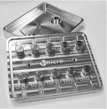
Spectroscopy and images with SNOM tips that have been packaged in standard AFM Gel-Pak boxes can lead to artifacts in the optical response. This is due to contamination of the tip by a few molecules of the gel. Vmicro has developed a back-end process with special decontamination and storage in a metal box. You can select this feature as an option when selecting your reference.


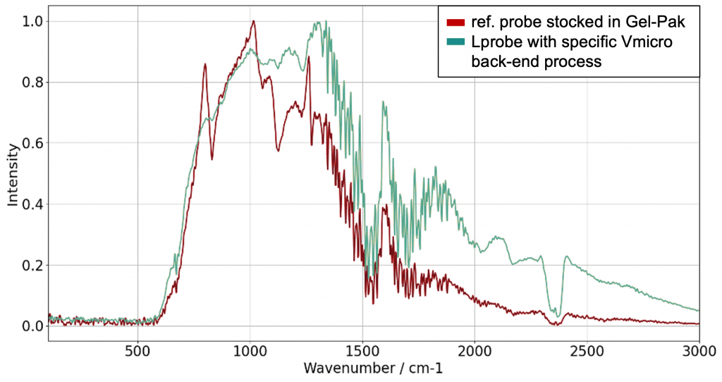
Nano-FTIR spectra normalized and obtained at the SMIS beamline at Synchrotron SOLEIL. (Courtesy F. Borondics – G. Németh)

Find probes by application

Conductive

Electrical measurements

s-SNOM

s-SNOM Probes for IR

Platform Cantilevers

Tilt compensated flat surface